
Views: 427 Author: Site Editor Publish Time: 2022-12-13 Origin: Site

Why do some wafers have no chips on the outer ring, while some wafer circuits spread the entire silicon wafer, and there will be incomplete chips on the outer ring of the wafer?
Friends who are familiar with the semiconductor manufacturing process know that before the chip is cut and packaged, all the manufacturing processes are performed on the wafer (Wafer). However, the chips we see are all square. When chips are manufactured on round wafers, there will always be some areas that are not used. So why not use square wafers to increase utilization?
We always ridicule that chips are essentially a pile of sand, and this sentence is not wrong. The basis of making chips - single crystal silicon is made from quartz sand.
The key to turning sand into chips lies in the purification of silicon and the development of single crystal silicon preparation technology. In 1916, Polish chemist Tchaikovsky accidentally dipped his pen into a tin crucible instead of an ink bottle. He immediately pulled out the pen and found a solidified wire hanging from the nib. Tchaikrasky verified through experiments that this metal wire is composed of a metal single crystal, and the diameter of the single crystal reaches the millimeter level. Since then, the method has been continuously iterated by chemists, and finally single crystal silicon has been made. This method is also known as the Tschakelsky method or the Czochralski method. Single crystal corresponds to polycrystal, which is composed of many small crystal grains, and the arrangement of crystal grains is not regular. A single crystal itself is a complete large grain, and the atoms or ions in the crystal are arranged in an orderly manner. Since polysilicon does not have repeated single-crystal structures to provide stable electrical and mechanical properties like single-crystal silicon, the silicon wafers used to make chips can only be single-crystal silicon.
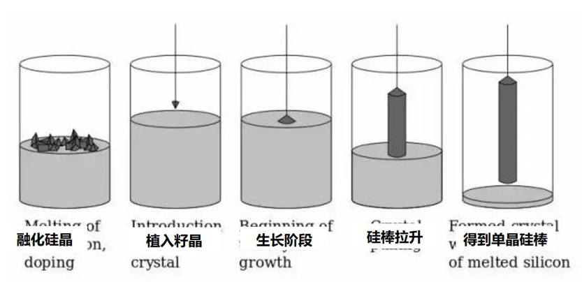
The process of the Czochralski method is to heat high-purity silicon into a molten state in a crucible, then place a seed crystal (seed crystal) at the end of a precisely oriented rod, and immerse the end in molten silicon, and then place the rod Slowly pull up and rotate. Through the precise control of the pulling rate, rotation rate and temperature, a large cylindrical single crystal silicon rod can be obtained at the end of the rod, and after the silicon rod is polished, polished, cut and other processes, it can be Got a usable round silicon wafer. Therefore, the roundness of the wafer is due to the "roundness" of the silicon rod. But to be precise, the wafer is not completely round. Usually, after the silicon wafer is processed into a wafer, a gap will be ground around it (a flat angle will be cut below 200mm, and a small opening will be cut above 200mm to avoid waste). This is to mark the growth direction of the silicon crystal and facilitate subsequent photolithography. 1. Positioning the wafer in the etching step.

cut silicon rods
In fact, the silicon rod can be cut into a cuboid before slicing, so that the "crystal cube" can be obtained directly in the subsequent slicing. But the silicon rods used to make chips don't do this, for several reasons:
The first is that the round shape is more suitable for photolithography coating. Before photolithography, a layer of photoresist needs to be evenly coated on the surface of the wafer. The uniformity of the coating directly affects the yield of the chip. commonly used gluing method is to smear the glue in the center of the silicon wafer, and then shake off the photoresist and spread it over the entire wafer by rotating. Due to the viscosity of the liquid, surface tension and air resistance, photoresist accumulation will Occur at the four corners of the square wafer after the glue is thrown, which will eventually affect the overall photolithography effect, resulting in a decrease in yield and more waste.
In addition, due to the presence of edge stress, the structural strength of circular wafers is also higher than that of square wafers. Before the silicon wafer becomes a wafer, it needs to undergo multiple processes such as photolithography, etching, and chemical polishing, and the wafer will accumulate more stress on the outer ring. Therefore, the sharp corners of the square will cause stress concentration at the edge, which is easily damaged during the production process and affects the overall yield.
Careful friends may find out why there are no chips in the outer ring of some wafers, while some wafer circuits spread the entire silicon wafer, and incomplete chips appear in the outer ring of the wafer?

Wafer outer rings vary
This is actually related to the size of the photomask (Mask, or mask, photolithography plate) in lithography. The essence of photolithography is to expose the silicon wafer coated with photoresist to specific light (such as EUV extreme ultraviolet light), and the light will leave the required circuit pattern on the surface of the wafer after passing through the photomask. The photomask itself is square, and it consists of many grids. Each grid is called a shot, which is the smallest unit of exposure. Shot includes one or more Dies and peripheral test circuits. Shot is square, so Die is also square. The photomask size usually covers the entire area of the wafer, so there will be small incomplete squares at the edge of the wafer. In addition, due to the edge effect, if the peripheral circuits are not fabricated after photolithography, the material density inside and outside the circle will be affected, which in turn will affect the overall yield. Industry insiders explained this phenomenon: "In the chip manufacturing process, the wafer is constantly thickened, especially the back-end metal and through-hole manufacturing process, which will use multiple CMP chemical mechanical polishing processes. If the wafer There is no pattern on the round edge, which will cause the edge grinding rate to be too slow, and the height difference between the edge and the center will affect the adjacent complete chip in the subsequent grinding process. Therefore, even as a dummy pattern, the incomplete edge All shots need normal exposure.”
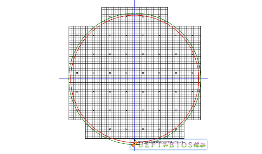
The green circle is the wafer area, and the red circle is the usable part
However, the chips on the outer ring of the wafer are generally not used. As mentioned above, due to the relationship between the production process, there must be some stress on the periphery of the wafer. The chips produced here will also retain stress inside, and there is a greater probability of chip damage during the subsequent cutting, packaging, and transportation. damage. Therefore, at present, when manufacturers use large-area wafers to produce chips, they will choose to cover the entire wafer with circuits to improve the yield rate. This is also the reason why some wafers have chips on the outer ring, and some do not.
In general, round wafers are more convenient for chip manufacturing and have a higher yield. Since the wafers used to make chips are inconvenient to make square, why can't chips be made round?
After silicon wafers go through steps such as gluing, photolithography, etching, and ion implantation, chips will be manufactured one by one. However, at this time, the chips are still "grown" on the wafer and need to be cut to become a single chip. individual chips.
Imagine a square chip that could be cut out entirely with just a few knives. What about round chips? I'm afraid it will take several times longer than the square to cut. From the packaging direction, the square chip is also convenient for wire operation. Even if it is a Flip chip package, the square shape is more convenient for the machine to operate the chip to align the I/O interface with the pad.
The most important point is that circular chips cannot solve the problem of wasting silicon wafer area. Cutting many square areas on a wafer, these areas will not have gaps in the middle, only leaving gaps at the edge of the wafer. However, if many circular areas are cut from a plane, some areas in the middle will be wasted, and the waste of the periphery of the wafer cannot be avoided.
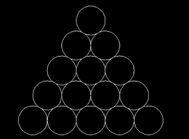
There will be gaps in the circular arrangement
In fact, saving wafer area is always an important issue. The more chips that can be produced on a wafer, the higher the production efficiency and the lower the cost of a single chip. At present, the best way to solve production efficiency is to increase the wafer area, which is the calculus we are familiar with.
The larger the wafer, the smaller the free area
It can be easily seen from the picture that when the chip area is fixed, using a larger wafer can effectively improve the utilization rate of the wafer. According to the calculation formula commonly used by Fab factories in the world:

A 100mm² chip on a 12-inch wafer can produce about 660 chips, while using an 8-inch wafer, there are only 180 chips. The wafer area is reduced by 50%, but the number of chips is 72% less. Therefore, the current 12-inch wafer has become the main battlefield for the world's largest IDM and foundry manufacturers.
From the perspective of wafer utilization, it is impossible to have round chips at present, but square "wafers" do exist, not only exist but also very common. In addition to making chips, silicon wafers are also an extremely important part in the field of photovoltaics.
Photovoltaic power generation is a form of power generation that uses the photovoltaic effect of silicon wafers to directly convert sunlight radiant energy into electrical energy. The photovoltaic effect of crystalline silicon is applicable to both polycrystalline and single crystal, but monocrystalline silicon has complete crystals, uniform optical and electrical properties, higher mechanical strength, and more efficient photoelectric conversion, so the conversion efficiency of single crystal cells can be 2 times higher than that of polycrystalline cells -3 percentage points.
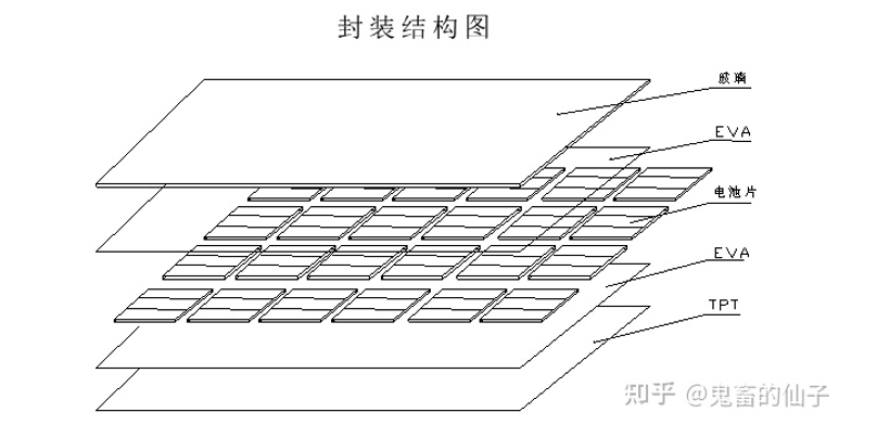
Solar panel structure (batteries are silicon wafers)
The early stage of the preparation process of photovoltaic monocrystalline silicon is the same as that of chip monocrystalline silicon. First, the high-purity silicon is heated to a molten state, and then a single crystal silicon rod is pulled out from it. Before slicing, photovoltaic silicon will first cut the silicon rod into a cuboid, so that the cross section of the silicon wafer becomes a square. The reason for using a square shape is also very simple. If the photovoltaic cell is circular, there will be gaps in the middle of the solar panel when multiple cells are arranged, which reduces the overall conversion rate.
Compared with chips, the requirements for the purity of silicon in the manufacture of photovoltaic panels are slightly lower, and the purity standard only needs to be 99.9999%, which cannot reach 99.999999999% for making chips.
Summarize
To answer the question posed by the title, why is the chip square? Circular chips are difficult to cut, and the subsequent packaging stage is not easy to control. Most importantly, circular chips cannot solve the problem of wasting wafer area. Why are wafers round? In the process of chip production, circular wafers are more convenient to produce due to mechanical factors, and the yield rate is higher, and silicon rods are naturally cylindrical, and wafers are naturally circular. However, in the field of photovoltaics, square silicon wafers do not waste space when packaging cells, so photovoltaic silicon wafers are square.


