
Views: 0 Author: Site Editor Publish Time: 2025-02-07 Origin: Site
Why do we need to polish the wafer so smoothly?
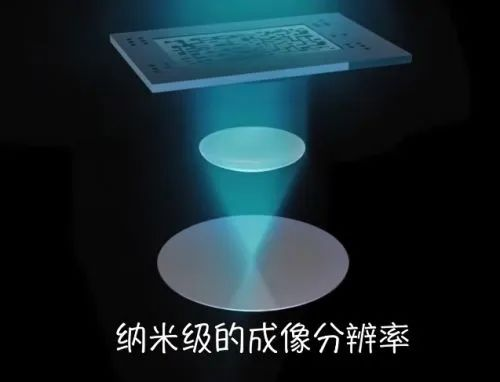
The final fate of the wafer is to be cut into chips (die), packaged in a dark box, with only a few pins exposed. The chip will look at the threshold, resistance, current value, and voltage value, but no one cares about its appearance. In the process, we repeatedly polish the wafer to meet the flattening needs in production, especially when doing photolithography, the surface of the wafer must be extremely flat. This is because as the chip process shrinks, the lens of the photolithography machine must desperately increase the numerical aperture of the lens to achieve nanometer-level imaging resolution, but this will also lead to a decrease in the depth of focus (DoF). The depth of focus refers to the focusing depth of optical imaging. In order to ensure that the photolithography image is clear and not out of focus, the ups and downs of the wafer surface must fall within the range of the depth of focus.
Simply put, in order to improve imaging accuracy, the lithography machine sacrifices focusing ability. For example, the new generation of EUV lithography machines has a numerical aperture of 0.55, but the vertical focal depth is only 45 nanometers in total, and the optimal imaging range during lithography will be even smaller. If the wafer placed on it is not flat enough, the thickness is uneven, and the surface is undulating, it will cause problems in the lithography of the high and low places.
Of course, it is not only photolithography that requires a smooth wafer surface. There are many chip manufacturing processes that require polishing the wafer. Polishing is required after wet etching to tighten the rough surface of the corrosion to facilitate glue deposition. Polishing is required after shallow trench isolation (STI) to grind off excess silicon oxide to complete trench filling. Polishing is required after metal deposition to remove the overflowing metal layer to prevent device short circuit. Therefore, the birth of a chip requires many polishings to reduce the roughness and ups and downs of the wafer and remove excess surface substances. In addition, various process problems on the wafer cause surface defects, which are often exposed only after each polishing is completed. Therefore, the engineers responsible for polishing have a heavy responsibility. They are not only the C position in the chip manufacturing process, but also the T position in the production meeting. They must be able to wet etch and understand physical output.
What are the polishing methods for wafers?
The polishing process can be divided into the following three categories in principle according to the interaction between the polishing liquid and the silicon wafer surface.
![]()
1. Mechanical polishing method
Mechanical polishing is a polishing method that obtains a smooth surface by cutting and plastic deformation of the material surface to
remove the convex parts after polishing. Generally, oil stone strips, wool wheels, sandpaper, etc. are used, and manual operation is the main method. Special parts such as the surface of a rotating body can use auxiliary tools such as a turntable. For special parts such as the surface of a rotating body, ultra-fine grinding and polishing can be used. Ultra-fine grinding and polishing is to use a special grinding tool, which is pressed tightly on the surface of the workpiece in a grinding and polishing liquid containing abrasives and rotates at high speed. Using this technology, the surface roughness of Ra0.008μm can be achieved, which is the highest among various polishing methods. Optical lens molds often use this method.
2. Chemical polishing method
Chemical polishing is to make the microscopic convex parts of the material surface in the chemical medium dissolve preferentially over the concave parts, thereby obtaining a smooth surface. The main advantages of this method are that it does not require complex equipment, can polish workpieces with complex shapes, can polish many workpieces at the same time, and is highly efficient. The core issue of chemical polishing is the preparation of polishing liquid. The surface roughness obtained by chemical polishing is generally several tens of μm.
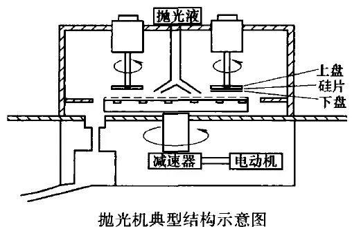
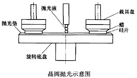
3. Chemical Mechanical Polishing (CMP)
The first two polishing methods have their own unique advantages. If these two methods are combined, the advantages and disadvantages can be complementary in terms of process. Chemical mechanical polishing uses a process that combines mechanical friction and chemical corrosion. During the CMP process, the chemical reagents in the polishing liquid used for CMP will oxidize the polished base material to form a softer oxide film layer, and then remove the oxide film layer through mechanical friction. In this way, through repeated oxidation film-mechanical removal processes, the purpose of effective polishing is achieved.
The current chemical mechanical polishing (CMP) field faces some challenges and problems, including technical, economic and environmental sustainability aspects:
(1) Process consistency: Achieving high consistency in the CMP process remains a challenge. Even on the same production line, there may be slight differences in process parameters between different batches or between different equipment, affecting the consistency of the final product.
(2) Adaptability to new materials: As new materials continue to emerge, CMP technology needs to constantly adapt to the characteristics of new materials. Some advanced materials may not be compatible with traditional CMP processes, and more adaptable polishing liquids and abrasives need to be developed.
(3) Size effect: As the size of semiconductor devices continues to shrink, the problems caused by size effect become more significant. At micro-sizes, the requirements for surface flatness are higher, so more precise CMP processes are required.
(4) Material removal rate control: In some applications, precise removal rate control of different materials becomes particularly critical. Ensuring the consistency of removal rates of different layers of materials during the CMP process is crucial to manufacturing high-performance devices.
(5) Environmental friendliness: The polishing liquids and abrasives used in the CMP process may contain some environmentally harmful components. Researching and developing more environmentally friendly and sustainable CMP processes and materials is an important challenge.
(6) Intelligence and automation: The intelligence and automation of CMP systems are gradually improving, but they still need to cope with complex and changing production environments. How to achieve a higher degree of automation and intelligent monitoring to improve production efficiency is a problem that needs to be solved.
(7) Cost control: The CMP process involves high equipment and material costs. Manufacturers need to strive to reduce production costs while improving process performance to maintain market competitiveness.


