
Views: 0 Author: Site Editor Publish Time: 2025-02-14 Origin: Site

Silicon wafers are the carriers of most chips. But a piece of silicon wafer hides many unknown details, such as: What are the crystal orientations of silicon wafers? How many positioning flats are there? How is the positioning flats positioned? What is the difference between the positioning flat and the positioning notch? How do they interact with each other? And so on. Let's explain it in detail today.
Wafer Flat
The wafer flat refers to the flat part on the outer of the wafer. It is used to mark the specific direction of the wafer to ensure that the wafer can be properly aligned during the processing and handling of the wafer. You can think of it as a compass needle to help guide the correct placement of the wafer in the equipment. Usually, the positioning (flat) is used for positioning silicon wafers below 8 inches. The silicon wafer positioning flat is a short side of the silicon wafer.
Function and role:
Direction indication: The positioning flat usually shows the specific crystal plane direction of the wafer. For example, for a P-type <100> crystal orientation silicon wafer, the positioning flat can help indicate its main direction. This is because the silicon crystal structure of different crystal orientations has different physical and electrical properties, and the role of the wafer positioning flat is to ensure that the crystal orientation is correctly identified during wafer processing.
Alignment mark: In wafer manufacturing, multiple steps of alignment operations are required, such as lithography alignment, etching alignment, etc. The positioning flat is like a coordinate mark on a map, which helps the equipment align the wafer position and ensure processing accuracy.
Example metaphor: The positioning flat of the wafer can be compared to the indicator lines in a puzzle, telling us how to correctly splice the various parts. Without these indicator lines, we may not be able to complete the puzzle correctly.
Wafer Notch

A wafer notch is a small cut or notch on the outer of the wafer. This notch is similar to the positioning flat and also has the function of marking the direction of the wafer, but its shape and function are different. Usually, the notch is a physical notch, while the positioning flat is straight.
Function and role:
Precise positioning: The notch is often used to provide more precise direction identification, especially in larger wafers (such as 300mm wafers). The notch allows manufacturing equipment to more easily identify the direction of the wafer and avoid alignment errors caused by rotation or slight movement of the wafer.
Avoid alignment errors: The notch, as a marker, can help automated equipment more stably keep the direction of the wafer consistent throughout the processing process. It reduces human errors and improves production efficiency.
Example metaphor: You can compare the notch to the position of the valve of a car tire. Although it does not affect the rotation of the tire, it is a key point for positioning the tire and ensures that the tire can be accurately installed.
Relationship between wafer positioning flat and notch:
Wafer positioning flat and notch complement each other in the wafer manufacturing process. The positioning flat provides a rough direction indication for the wafer, while the notch provides a physical mark for further precise positioning. Both exist simultaneously in most applications, especially in large-size wafers (such as 300mm wafers)
How are the Notches/Flats made?
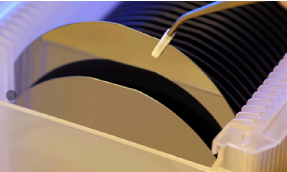
After the CZ method is used to pull out the ingot, the two ends need to be cut off, and then the silicon ingot needs to be radially ground to obtain a suitable diameter. Then a part of the silicon ingot is ground to obtain the positioning flat, and finally the silicon ingot is cut into silicon wafers with a wire saw or an inner circle cutter.
Relationship with crystal orientation & doping
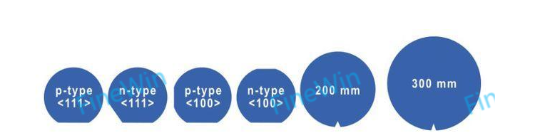
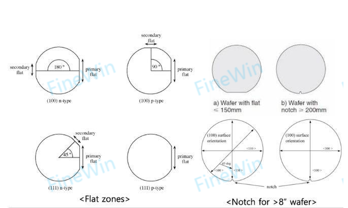
Generally, only the positioning flat has the function of indicating the crystal orientation and doping type. The crystal orientation and doping type of the silicon wafer are determined according to the position and number of the positioning flats. The positioning notch will be at the bottom of the silicon wafer, and the crystal orientation and doping type cannot be intuitively seen through the positioning notch. Common crystal orientations are <100>, <110>, <111>, and the doping types are N-type and P-type.
The number of positioning flats of a silicon wafer is one or two. The type of silicon wafer with only one positioning flat is P-type <111>. If the silicon wafer has two positioning flats, then the longer positioning flat is the primary positioning flat, and the shorter one is the secondary positioning flat. The main positioning flat is mainly used to facilitate the alignment of silicon wafers in the semiconductor process, while the secondary positioning flat indicates the crystal orientation and doping type. The main positioning flat is at the bottom of the silicon wafer, while the position of the secondary positioning flat is not fixed and changes with the crystal orientation and doping type of the wafer.
Generally, the length of the main positioning flat of a 2-inch silicon wafer is 15.8mm, the length of the main positioning flat of a 4-inch silicon wafer is 32.5mm, and the main positioning flat of a 6-inch silicon wafer is 57.5mm. When the angle between the main positioning flat and the secondary positioning flat is 45°, the silicon wafer type is n-type <111>; when the angle between the main positioning flat and the secondary positioning flat is 90°, the silicon wafer type is p-type <100>; when the angle between the main positioning flat and the secondary positioning flat is 180°, the silicon wafer type is n-type <100>. Since the <110> crystal orientation is not a mainstream silicon wafer crystal orientation, there is no standard to indicate it. The <110> crystal orientation can be indicated according to the silicon wafer supplier's own standards.
The influence of crystal orientation on semiconductor processing: On the (100) crystal plane, the arrangement of silicon atoms is tetragonal, while on the (111) crystal plane, the arrangement of silicon atoms is hexagonal. Since the silicon atoms on the (111) crystal plane are more compact, their chemical reactivity is relatively low, while on the contrary, the (100) crystal plane has a higher chemical reactivity. Therefore, silicon on the (100) crystal plane etches faster than silicon on the (111) crystal plane, and the oxidation rate of the (111) crystal plane is usually lower than that of the (100) crystal plane.
The influence of silicon wafer doping concentration on semiconductor processing:
During the etching process, dopants increase the conductivity of silicon, making it more susceptible to electrochemical etching. Different doping concentrations will result in different etching rates, and highly doped silicon will usually etch faster. In the diffusion process, the doping concentration of the silicon wafer will also affect the diffusion rate of dopants in silicon. Highly doped silicon will cause dopants to diffuse deeper.


