
Views: 13 Author: Site Editor Publish Time: 2022-01-19 Origin: Site
The production of silicon wafers usually has the following steps:
1) Crystal growth can be divided into Czochralski method (CZ) and zone fusion method (FZ). Since the molten polycrystalline material will directly contact the quartz crucible, the impurities in the quartz crucible will contaminate the molten polycrystalline. The content of crystalline carbon and oxygen is relatively high, and there are many impurity defects, but the cost is low. It is suitable for drawing large-diameter (300mm) silicon wafers and is currently the main semiconductor silicon wafer material. The single crystal drawn by the zone melting method has few internal defects and low carbon and oxygen content because the polycrystalline raw material is not in contact with the quartz crucible.
2) Slicing, the drawn single crystal silicon rod needs to be cut off from the head and tail, then rolled to the required diameter, cut into flat edges or V grooves, and then cut into thin silicon wafers. At present, diamond wire cutting technology is usually used, which has high efficiency and good warpage and curvature of silicon wafers. A small number of special special-shaped pieces will be cut with inner circle.
3) Grinding: After slicing, it is necessary to remove the damaged layer on the cutting surface by grinding to ensure the quality of the surface of the silicon wafer, and remove about 50um.
4) Corrosion: Corrosion is to further remove the damage layer caused by cutting and grinding in order to prepare for the next polishing process. Corrosion usually includes alkali corrosion and acid corrosion. At present, due to environmental protection factors, most of them use alkali corrosion. The removal amount of corrosion will reach 30-40um, and the surface roughness can also reach micron level.
5) Polishing: Polishing is an important process in the production of silicon wafers. Polishing is to further improve the surface quality of silicon wafers through CMP (Chemical Mechanical Polished) technology to meet the requirements of production chips. The surface roughness after polishing is usually Ra<5A.
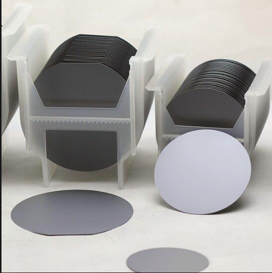
6) Cleaning and packaging: As the line width of integrated circuits is getting smaller and smaller, the requirements for improved particle size indicators are also getting higher and higher. Cleaning and packaging is also an important process in the production of silicon wafers. Most of the particles above 0.3um on the wafer surface are then vacuum-sealed and packaged in a no-clean jam box or packed with inert gas, so that the cleanliness of the wafer surface can meet the requirements of integrated circuits.
Monocrystalline silicon is an excellent high-purity semiconductor material. The purity of IC grade is required to reach more than 9N (99.9999999%), and the zone melting single crystal silicon wafer even reaches more than 11N (99.999999999%). It is usually obtained by Czochralski (CZ) and zone fusion (FZ) growth, and its crystallographic orientation is determined by the seed crystal. Monocrystalline silicon is currently the most important semiconductor material, accounting for more than 90% of the semiconductor material market, and is the basic material for information technology and integrated circuits.


