
 |
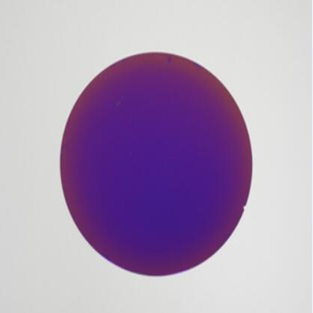

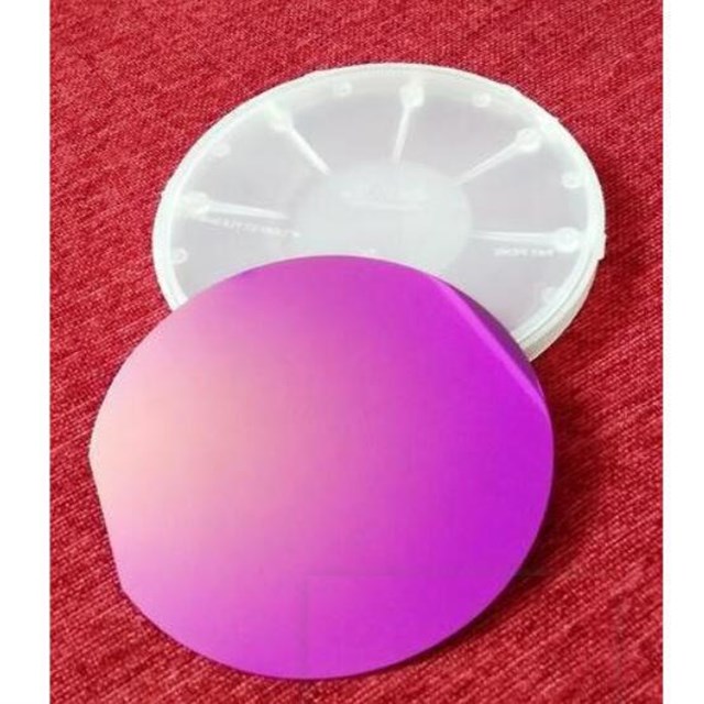
Within the semiconductor industry, silicon nitride layers are used as dielectric material, passivation layers or can act as hardmask. Additionally, there are several applications in micro-mechanics, for example as membrane material.
FineWin
Products specifications:
| Growth Method | CZ or FZ | |
| Type(doping) | P-type (B doped) or Ntype (P doped) | |
| Orientation | (100) | |
| Diameter | 2inch, 3inch, 4 inch | |
| Thickness | 200~800 μm, | |
| Surface | SSP (SiN on both side or on one side) DSP(SiN on both side) | |
| SiN film thickness | 100nm~500nm | |
| TTV&BOW | '≤25 μm | |
| Resistivity | 0~1000 ohm.cm | |
| Cleaning/ packaging | Vacuum packaging, 25 pieces in one cassette packaging | |
| Stock situation | your required specification can be sent to us for checking | |
