
 |


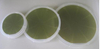
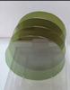

Currently, there are two main types of SiC wafers. The first type is the polished wafer, which is a single silicon carbide disc. It is made of high-purity SiC crystals, and can be 100mm or 150mm in diameter. It is used in high-power electronics. The second type is the epitaxial crystalline silicon carbide wafer. This type of wafer is created by adding layers of single silicon carbide crystals to a surface. This method requires precise control of the thickness of the material, and is referred to as n-type epitaxy.
A SiC wafer is a semiconductor material that has excellent electrical and thermal properties. It is a high-performance semiconductor that is ideal for a wide variety of applications. In addition to its high thermal resistance, it also features a very high level of hardness. Compared to other semiconductors, a silicon carbide wafer is ideal for a wide range of power and voltage applications. This means that it is suitable for a variety of electrical and optical devices.
Electric Vehicles (EVs): For traction inverters, onboard chargers, and DC-DC converters.
Renewable Energy: Inverters for solar panels and wind turbines.
Industrial Systems: Motor drives and high-power equipment.
Aerospace and Defense: High-efficiency power systems in harsh environments.
FineWin wafers provide domestic High quality Conductive (Conductive), Semi-insulating (Semi-insulating), HPSI (high Purity semi-insulating) silicon carbide substrate.
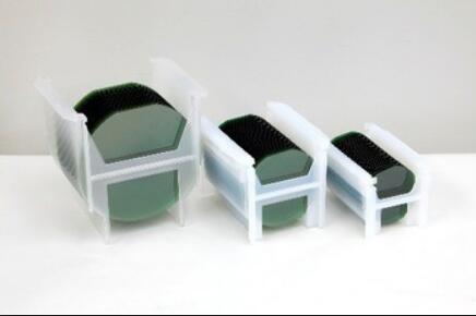
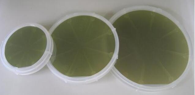
The Specification of SiC wafers we can provide.
1. 4H 4inch Ntype SiC wafers
2. 4H 4inch SItype SiC wafers
3. 4H 6inch SItype SiC wafers
4. 4H 6inch Ntype SiC wafers
5. 4H 8inch SItype SiC wafers
6. 4H 8inch Ntype SiC wafers

