
 |

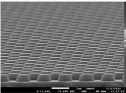
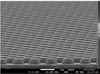

The formation of LEDs on patterned sapphire substrates is the most cost-effective method for manufacturing such devices. These LEDs exhibit high-normalized electroluminescence intensity and high light extraction efficiency. In addition, patterned wafers reduce defect density and total internal reflection losses. These advantages are driving the adoption of nitride-semiconductor-based LEDs by manufacturers.
Features:
Nano-scale pattern is available
Dome, pillar or rod types are available
Custom pattern is welcome
FineWin
6inch Cplane Patterned Sapphire Substrate (PSS)
Detailed specification:
| Crystal Material | 99.996%,high purity, monocrystalline Al2O3 |
| Grade | Prime |
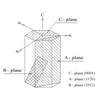
| Orientation | Cplane to Mplane |
| Diameter | 6 inch |
| Patterned Spec | Diameter: 2.7 ± 0.15 μm; Spacing: 0.3 ± 0.15 μm; Depth: 1.75 ± 0.15 μm |
| Pattern type | 3μm pitch, Cone Type |
| Thickness | 1000±25 μm |
| back Surface | fine ground |
| TTV/BOW/WARP | ≤ 25 μm |
| Package | Class 100 clean room cleaning, vacuum packaging; 25 pieces in one cassette packaging or individual packaging |
Application:
Currently, patterned sapphire substrates are most often used for the production of semiconductor GaN epitaxial light-emitting diodes. The use of patterned sapphire substrates in this process is increasing due to the varying chemical resistance of the material.
