
 |


SiC devices have irreplaceable advantages in the field of high temperature, high pressure, high frequency, high power electronic devices and extreme environmental applications such as aerospace, military, nuclear energy, etc., make up for the defects of traditional semiconductor material devices in practical applications, and are gradually becoming the mainstream of power semiconductors.
Compared with the first and second generation semiconductor materials, the third generation semiconductor materials have the advantages of high thermal conductivity, high breakdown electric field, high saturated electron migration rate and high bonding energy, which can meet the new requirements of modern electronic technology for high temperature, high power, high pressure, high frequency and radiation resistance and other harsh conditions. It has important application prospects in the fields of national defense, aviation, aerospace, oil exploration, optical storage, etc., and can reduce energy loss by more than 50% in many strategic industries such as broadband communications, solar energy, automobile manufacturing, semiconductor lighting, and smart grid, and can reduce equipment volume by more than 75%, which is of milestone significance for the development of human science and technology.
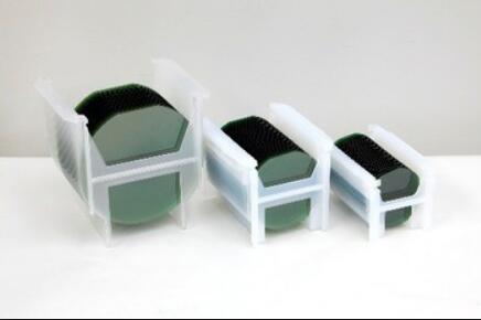
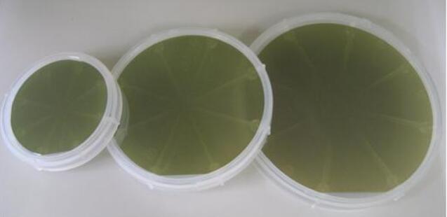
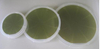
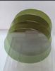
FineWin wafers provide domestic High quality Conductive (Conductive), Semi-insulating (Semi-insulating), HPSI (high Purity semi-insulating) silicon carbide substrate.
The Specification of SiC wafers we can provide.
1. 4H 4inch Ntype SiC wafers
2. 4H 4inch SItype SiC wafers
3. 4H 6inch SItype SiC wafers
4. 4H 6inch Ntype SiC wafers
5. 4H 8inch SItype SiC wafers
6. 4H 8inch Ntype SiC wafers

