
 |

The development of patterned sapphire substrates is expected to benefit the high-brightness LED industry.
Using Patterned Sapphire Substrates can significantly increase the light output of LEDs. Benefits include:
- Increased light emissions of active quantum well layers as the result of reduced epitaxial defect density.
-PSS reduces light loss due to the Total Internal Reflection (TIR) phenomena by enabling a photon scattering effect.
FineWin
Detailed specification:
| Crystal Material | 99.996%,high purity, monocrystalline Al2O3 |
| Grade | Prime |
| Orientation | Cplane offto Mplane |
| Diameter | 4 inch |
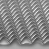
| Patterned Spec | Diameter: 2.7 ± 0.15 μm; Spacing: 0.3 ± 0.15 μm; Depth: 1.75 ± 0.15 μm |
| Pattern type | 3μm pitch, Cone Type |
| Thickness | 650±25 μm |
| Surface | SSP or DSP |
| TTV/BOW/WARP | ≤ 15 μm |
| Package | Class 100 clean room cleaning, vacuum packaging; 25 pieces in one cassette packaging or individual packaging |
Sapphire wafer is the most widely used substrate material in semiconductor lighting industry, and patterned sapphire substrate (PSS) is the general method to improve the luminous efficiency of semiconductor lighting devices. These sapphire substrates are with periodic structures of various shapes such as cone, dome, pyramid, and pillar, etc.
