
 |


Almost every electric device in our surroundings has silicon wafers in it. When it comes to making semiconductors, it is a pretty famous material. A flat-disk having a surface that's like a mirror and polished looks similar to the silicon wafer. An irregularity-free surface improves the purity of the surface, therefore making it a perfect candidate for the semiconductor devices
Products Specifications(General):
| Growth Method | CZ | |
| Type(doping) | P-type (B doped) or Ntype (P doped) | |
| Orientation | (100) or (111) | |
| Diameter | 2inch~12inch | |
| Thickness | 200~1500 μm, | |
| Surface | SSP or DSP | |
| TTV&BOW | '≤15 μm | |
| Resistivity | 0~300ohm.cm | |
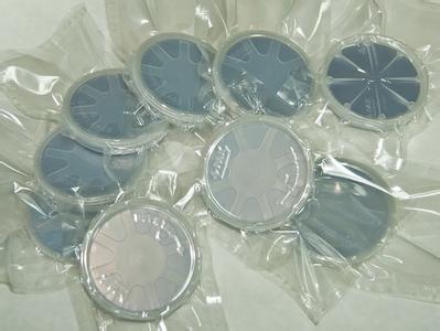
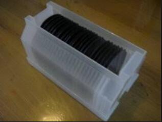
| Cleaning/ packaging | Vacuum packaging, 25 pieces in one cassette packaging | |
| Stock situation | your required specification can be sent to us for checking | |
